Amazon updated the Dash Button’s hardware to revision two earlier this year, so I decided it was time for a new teardown (here’s last year’s teardown). The new product number is JK29LP; the old product number is JK76PL. While the form factor and case remained much the same, the internals changed substantially. The major highlights are a switch from Broadcom to Atmel chips, a switch from an Energizer lithium battery to a Duracell alkaline battery, and the addition of Bluetooth Low Energy. to Old Dash Button (Bottom)")
After unboxing the new Button, the first change1 is visible, albeit minor—the design of the mounting adhesive on the back of the Button changed.


Removing the front label reveals another change, the removal of the three screws that were under the label. It turns out that they weren’t actually removed, just moved inside. The screws only hold the PCB to the case; they never held the case together. The new Button, like the old Button, needs to be pried open, which reveals the battery. The case is closed using ultrasonic welding.2


The original Dash Button contained a lithium battery that was tab-welded in place and thus rather permanent. The new button includes an alkaline battery in a holder; it’s still not really replaceable as one has to pry open and damage the case to get at it, but the holder is an improvement. Removing the three Torx T5 screws, the ones that used to be under the front label, allows one to remove the plastic around the battery and remove the PCB from the case.


This now allows us to inspect the PCB, which has the obvious change of blue solder mask instead of green solder mask like the original Button.


Instead of Broadcom chips, the new Button features an Atmel ATSAMG55J19A-MU ARM microcontroller, U1, and an Atmel ATWINC1500B wireless chip, U19. As a new addition, it also has a Cypress CYBL10563-68FNXI Bluetooth Low Energy chip, U22. The flash memory, U15, has been moved to the back of the PCB and doubled in size to 32 Mbit; it appears to be a Micron N25Q032 chip. The microphone was also swapped out, although I was unable to identify the new part. Finally, the microcontroller’s programming header is no longer populated, although it appears to be the same footprint, so it should be able to be populated with a Panasonic AXE510127 header. The new Button is likely easier to reprogram, since Atmel is much more forthcoming with documentation than Broadcom.
Since the new Button uses a lower capacity alkaline battery when compared to the original Button’s lithium battery, I analyzed the power usage of both Buttons. While in sleep mode, the new Button uses ~2.0 μA, down from the original Button’s ~2.3 μA. More interesting is the power usage when activated. The new Button uses slightly more power when on but uses less energy per button press, since it stays on for a much shorter period of time. The original Button shows the peculiar behavior of staying on for a long time after the LED turns off before going back into sleep mode,3 which accounts for the increased energy usage; it’s unclear to me whether this is due to the hardware design or due to the firmware. As I was having issues with my multimeter’s internal resistance causing a brown-out when the Button was pressed due to the current surge of the Button powering on, which would cause the Button to reset,4 there’s the chance the extended “on” time was due to my measurement setup, although I think this is unlikely. An example power usage graph for each Button is below. The triangle wave signal in the graphs is from the Button’s LED pulsating while the transaction is happening. There are mostly likely brief power usage spikes during RF transmission that aren’t visible in the graphs.
Using a sample size of five for each Button, I measured the new Dash Button’s energy usage to be 4.3±2.2 J per activation and the original Button’s energy usage to be 16.4±0.1 J per activation. According to the batteries’ corresponding datasheets, the new Button’s alkaline battery contains ~2 kJ, while the original Button’s lithium battery contains ~4.3 kJ. This corresponds to ~500 presses for the new Button and ~250 presses for the old Button. It turns out that the new Button should last longer despite having a cheaper, lower capacity battery.
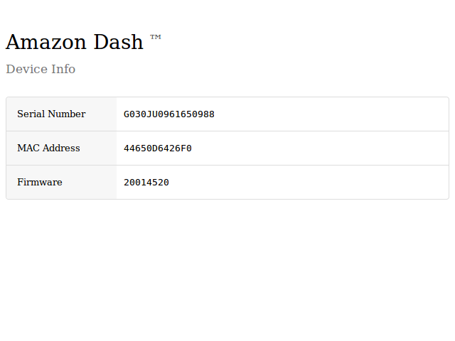
Moving on to the software and firmware, Bluetooth is now the primary means of configuring the Button; when placed in configuration mode, the Button is discoverable as a Bluetooth Low Energy device with name DashButton and a random MAC. The previous configuration mechanisms, Wi-Fi for Android and ultrasound for iOS, serve as fallbacks. The device’s web page, which can be accessed by connecting to the Amazon ConfigureMe network has changed. It no longer contains a form for entering network configuration information and instead lists the Button’s serial number, MAC address, and firmware version (it now uses CSS styling, too). Sniffing the setup sequence revealed some information on how the setup protocol works. The Android app first issues a GET request for http://192.168.0.1/, which is presumably to determine the model number and firmware version. It then issues the same request but with the Content-Type: application/json header set; the Button now returns a JSON file than contains the Button’s serial number, MAC address, and a list of visible Wi-Fi networks and their signal levels. This is an improvement as the app now shows the networks the Button can see instead of those the mobile device can see. The app then issues a GET request along the lines of http://192.168.0.1/token?value=o%26vD, where the four-byte value changes every time; I don’t know where it comes from. Next, another GET request is made for http://192.168.0.1/. Finally, the Button is configured using a GET request for http://192.168.0.1/?amzn_ssid=SPECIFIED_SSID&amzn_pw=SPECIFIED_PASSWORD, where SPECIFIED_SSID and SPECIFIED_PASSWORD correspond to the SSID and password entered into the app. Unfortunately, the new Button can’t easily be set up using a laptop like the old button could.
Overall, the new Dash Button appears to be a revision designed to reduce production cost, centered around a reduction in energy usage, which allows for use of a considerably cheaper, alkaline battery.
While removing the gunk surrounding the Atmel chip, there is a small chip labeled U23. Interesting little chip. First off it appears to be a BGA chip, even though it’s about the size of a SOT23. It also has a extremely thin coating on it used for the package. Just looking at it wrong will cause it to flake off leaving the top of what I assume to be a bare die. Unfortunately a tiny bit chipped off and of course it contains the chip markings so I can’t determine what it is. If you attempt to remove the gunk around the Atmel chip (it’s some kind of rubber) that chip is at the top, to the left of the pink pin one marker on the Atmel chip. It’s under the rubber so be extremely careful in this area. Let me know if you can get a part number off of it. Also if you brave removing the rubber to get at the pin connections, there are a lot of smd resistors, caps, etc. buried in that stuff so slow and steady!
I haven’t looked at it closely, but it’s probably a WLCSP package, which is essentially an unencapsulated diced silicon wafer with solder balls on the bottom.
There are markings on it, it has a thin coating on it that has the markings. All I can see thought is the letter “C”, the rest has flaked off
On mine it looked like it read
C0
ATE
but that’s a bit of a guess.
What’s for certain though, is that the part is essential to functionality.
After it’s damaged, a button press makes the LED come on blue for as long as the battery lasts.
One of the pins connects to PA7 (Pin 11) of the Atmel.
Hey Lonnie are you working on a schematic? Are you posting your results anywhere?
Hi,
I think that the chip you are referring to is a ATECC108.
This is a crypto chip used for security, authentication and ciphering.
You can see it on the WINC1500-XPRO evaluation board.
One of the package variant is a 3-lead (SOT-23 like) package.
Not meaning to spam your post but if you look just below u15, you’ll see what looks like a jtag connector solder mask. It is not populated, but it does look like it’s hooked up to the board. This connector was populated on the rev01 board…
I agree that this is probably JTAG and appears to be connected (it’s mentioned in the post).
Yea I saw it after I posted, so sorry about that. From what I’ve gathered from my limited probing, if you hold the board so the jtag solder mask is to the left of the bottom chip, pin 1 is the upper left pin, which would leave the reset as the lower right pin. The reset is held low until the button is hit, then it is pulled high to take it out of the reset state.
That’s about all the info I have right now. Don’t have a jtag/ice debugger to hook up to that solder mask so I’ll have to order one and see what info I can get out of it. I doubt it will be as easy as the REV01, they used all chips with code/memory protection on them, but who knows, maybe the fuses aren’t set…
I have 99% of that rubber gunk scraped away from the atmel chip, there are a lot of tiny bare die chips, some with numbers, some without. I believe they are voltage regulators, and things along that line. They are also BGA (4 balls from what I can see). It would be way too much work to sort those out so I’ll just stick with the jtag header, see if I can get something out of it
Quoting the datasheet:
“The SAM G55 features a security bit, based on a specific general-purpose NVM bit (GPNVM bit 0). When the
security is enabled, any access to the Flash, SRAM, core registers and internal peripherals through the ICE
interface is forbidden. This ensures the confidentiality of the code programmed in the Flash.
[…]
Disabling the security bit can only be done by asserting the ERASE pin to 1, and after a full Flash erase is performed”
Which means that if I understood it right you might not be able to extract Amazon’s code, but erasing and reprogramming should be totally possible.
Unfortunately, the ERASE pin of the ATSAMG55 is connected to GND on the PCB, see this info:
http://key-basher.blogspot.de/2016/09/amazon-dash-button-version-2.html
I have read that the ATSAMG55 contains an I2C/SPI ROM bootloader. Maybe it would be possible to use that way to erase the firmware? But I don’t know if erasing the flash automatically would reset the security bit GPNVM bit0 to zero?
If the GPNVM bit1 (Boot Mode bit) is 0, the ROM bootloader should be accessible (via NRST toggling). When the ROM bootloader is active and an initial command is sent via I2C or SPI then the flash should be erased automatically. Maybe GPNVM bit0 would also be erased then and maybe JTAG would be accessible then?
Unfortunately I do not have an SAM ICE. Could anyone please try if you can read and change the GPNVM Bit1 via JTAG?
I read in a community post that “You can clear the GPNVM Boot Mode bit via Atmel Studio -> Device Programming menu”.
http://community.atmel.com/forum/entering-bootloader-atmel-samg55-xplained-pro
So what’s the plan to take over this device? See if there is a backup firmware image in the flash, disassemble it and figure out the OTA update mechanism and co-opt it to load a custom firmware? Figure out the schematics and use the ATSAMG55 to flash the cypress PROC? Then put a scripting engine on to become a programmable universal wifi/ble remote?
The OTA update mechanism presumably uses HTTPS, so it probably can’t be hijacked. There appears to be a JTAG header, so it should be able to be reprogrammed. That being said, I don’t really have enough interest to figure it out.
That’s unfortunate because it will leave a lot of people out of the game since they will not want to open the case, solder, etc… But good for Amazon I guess. Anyway, first step is schematic, or at least partial schematic. I don’t want to do all the work required either, but if there are a lot of people contributing I think it won’t be as daunting a task. Anyone suggest where we can collaborate on this? /r/dashbutton? I’m still waiting for some v2 buttons to arrive.
I wish I found your post before I bought a pile of these things.. but that being said they were only $0.99 each as opposed to the $19.99 for the AWS IoT version.
Anyone poke around and get the usb figured out yet?
I am sort of just getting into this, so pardon if my question doesn’t make sense.
I was reading your teardown for the JK76PL and saw that it has a microphone, but on the JK29LP it still appears to be a hole for the microphone. Do you know why that is?
There’s still a microphone on the new one; the part number just changed. The iOS app will use ultrasound to configure the Button if Bluetooth is disabled.
Agree with dashing. Let’s collaborate and get the pinouts.
Pingback: Bending The New Amazon Dash Button To Your Will | Hackaday
I think that the microphone (an ultrasonic smd sensor) is the metallic thing near on the bottom side of the pcb, near the top hole (marked MK2).
Any idea on why they use gunk on the Atmel chip?
You’re correct about the microphone. I’m not sure why the gunk is there.
That’s probably so you can not easily get to the pins of the Atmel.
Removing it bears the risk to damage important parts of the circuitry.
No, this is supposed to keep moisture away from the underside of the BGA. Removing it is totally possible but albeit difficult.
The MCU is not in a BGA but in a 64pin LQFP package. I just removed the gunk and found plenty of pins. Even some passives :)
Pingback: New Amazon Dash Buttons Using WINC1500 « Adafruit Industries – Makers, hackers, artists, designers and engineers!
U1 on the backside appears to be a 1.2/1.5V to 3.3V boost converter. I measured 3.3V on the C6 cap next to it. I would love to turn this into a mobile temperature sensor or mobile water detector/sensor.
After dealing with the damn glue they surrounded the part with, I was able to map out SWDIO, SWCLK, RST, GND, VCC(3.3V), UART_TX, and UART_RX.
The small 7 pad grid near C83 contains everything.
TX18 – SWDIO
TX19 – SWCLK
TX21 – 3.3V
TX20 – RESET
TX22 – GND
TX16 – UART TX
TX15 – UART RX
I am headed out to buy a case of beer for a friend that has a scope, who can hopefully solder lines to the pads (these are waaay smaller), then I will start working on getting my stlink and openOCD to talk to it.
If anyone has experience getting a Chinese knock off st-link V2 to talk to the SAMG55J19. If I get anywhere I will share.
Could you try to measure whether the 10 pads near J2/R277 on the back contain the same signal?
Hey there,
I have got an oscilloscope and an official Atmel In Circuit debugger. Currently I am looking into the Dash Button too, but I am having trouble with the tiny solder joints too.
Sorry for the late response. I didn’t test the other pads but I was able to get some 40awg lines on the pads. Using the stm32 debugger and openOCD I got the firmware off successfully. There is ALOT more there as compared to V1.
That sounds great. Would you share the firmware with us? After comparing it with a second dump for differences to avoid exposing information on your button id etc.
Hello everyone,
I am really interested to make the Amazon Dash v2 work. Therefore i have collected all the informations which i could found together and put them in one place:
https://github.com/EliasKotlyar/FreeDash
Feel free to contribute using a pull Request
PS: Can’t await to get all the things together to start developing. For now waiting for all the components (2x Amazon Dash, JTAG Debugger, Headers…)
Greetings
Elias
Do you know if the Breakout board for JTAG also fits the J2 header on the new Dash?
I hope it will fit and will report as soon as I get it.
Just thought I would drop this here: http://key-basher.blogspot.com/2016/09/amazon-dash-button-version-2.html
TLDR; I have placed the connector on Dash V2, the security bit is set on the Atmel, and asserting the ERASE pin is… interesting.
For this to work, you need to setup the button to connect to Amazon first? Anyway to avoid that?
It’s incredible how over-engineered this button is.
It contains THREE 32-bit CPUs. Two of them are ARMs.
Also, it appears the WiFi chip could actually be used for Bluetooth and the rest of the entire project.
It has more than enough RAM and Flash to deal with the entire Button Logic, the setup process and probably even the Audio decoding. I have no clue how Amazon can afford this without the companies paying a lot. They started saving on the battery but they never seem to have read any of the datasheets.
I want to estimate the manufacturing resource and energy demand for the dash button rev. 2.0 (lca – life cycle assessment). Therefore I need the entire list of electronic components. Has anyone figured out the schematic diagram and can post it here? Thanks! R.
If the ATSAMG55 erase pin is the solution in order to get the lock bit reset, it should be possible to lift the pin off the pad with some care and do a chip erase then. How to remove the rubber around the chip (at least around pin 3) without damaging the parts underneath? Has someone a good way?
I had the idea to try to lift off the erase pin (pin 3) of the MCU which should be possible with the LQFP package, in order to perform a full erase. I started to carefully remove the gunk. After I have removed the gunk and now after several hours the solder at the MCU pins became liquid at room temperature (similar like mercury, but a bit more solid). Is somebody else experiencing this?
I tried to sniff the Amazon ConfigureMe wifi/app.
It uses public keys now:
https://github.com/littleCdev/JK29LP-HTTPDump
Maybe this helps anyone.
I’m not an electrical engr/tech, but I’m trying to figure out how I might trigger this device to send its message on contact of two wires. I’m guessing that the small device under the bar code, and to the left of where it says “S1” is a momentary switch that is pressed on by the button? If so, can I just solder a wire to the two contacts on each side and when the wires contact each other that it will activate?
Yes, it is a momentary switch; your idea should work.
Hey Scott,
Have you tried soldering two wires to the S1 momentary switch? I’ve tried it on my side but no luck.
I guess I’m just too dumb to do it properly. Although I think that the actual connections are just underneath the button.
I want to know who’s the manufacturer of this tiny device?
Probably a contract manufacturer in China. I don’t actually know.
Thanks! Any idea about the cost?
No idea.
I guess I got the V2 button.. I can’t use the Amazon app, any ideas for setting these up?
I looked at the process a bit but never fully worked it out.
I actually found out you can just switch your country to USA or UK and the Prime button thing shows up if you scroll down far enough… I had signed up for a USA prime trial so I could setup my buttons, but even switching to UK where I wasn’t prime it let me enter the configuration mode… So hopefully this will work for anyone else outside the buttons home areas.
Also as far as reusing the button for something else, I found detecting the DHCP broadcast was the quickest way to catch the button (about 3 seconds)
Any suggestions on how to make the AWS IoT Button more waterproof for outdoor operation? IP53 or better would be fine. From the teardown images above, it looks to be fairly water-tight already, but Amazon doesn’t recommend using it in the rain. Even the little hole in the cover on the far end away from the button appears to have a rubber boot in the image.
Someone (maybe Amazon) should design and sell a protective silicone boot to go around the entire device, like you can buy for some PC keyboards. I hope I don’t need to invent it myself.
Lastly, Amazon appears not to offer any form of datasheet for this device. The datasheets for the 3 primary devices within it shown above indicate -40 capability, so that was a relief. Are there any other components that might prevent it’s use at subzero temperatures?
Stick it in some sort of plastic bag? Other than gluing the microphone hole on the end shut, I can’t think of any other way to make it more weatherproof. Since the case is ultrasonic welded shut, the microphone hole and the push button are the two potential points of moisture ingress.
The microcontroller, wireless chips, and flash memory are all rated to -40 degrees, so I suspect it will work. Passives are almost always rated that low. That just leaves the various power management ICs.
It looks like there may be a new version of the button. I received one with a completely different bottom. The actual adhesive it cut the same, but some of the printing (the amazon logo, the model number. FCC id, DSN, and a bit more) is under the adhesive.
I haven’t taken it apart to see if its just a change to the case, if I do I will try to take pictures, and make a post somewhere.
What’s the FCC ID? That should tell us if it is a new version or not.
I can support that claim. Mine looks as William described. The FCC ID in my case is 2AETK-1013. Same model number (JK29LP).
The FCC ID matches, so it’s not a new version.
Has anyone here tried the audio buffer overflow attack recently on the Amazon Dash v2? I’m trying to understand if my setup is bad or if they patched the vulnerability.
Recently ordered one of these and opened it up. A few things to note.
Opening : Unlike the older version, which used Torx screws on the outside under the label, mine was just glued. I used a blade to repeatedly score the joint and was eventually able to open it up.
Power : U1 is a TPS61201 3.3V boost regulator. Using a meter to check the connections, EN seems to be sourced by a FET or transistor on the other side of the board (U20), probably for soft start. C2 and C3 are input side filter caps, C5 and C6 are load caps. Can’t seem to measure either with my meter in situ, but I would expect C5 and C6 to be larger than the 10 uF referred to in the TI datasheet, and L is likely larger than 2.2 uH, due to the quick WINC1500 current ramp from a few mA to nearly 300 mA when connecting to an AP. Looks like PS is pulled high to Vin with 100 kOhm at R2, meaning that power save mode on this regulator is disabled.
Erase pin : According to the datasheet, the ERASE pin integrates a permanent pull-down so it can be left unconnected during normal operation. So, assuming a QFN package (-MU part number) maybe if you can wick the solder off that pad, the solder paste may have caused the package to float a little during reflow and there may be a gap between the QFN pad and the PCB pad (not sure about this, but here’s hoping). If LQFP (-AU part number) then it is much easier to wick the solder and lift the pin. This would enable you to briefly (5 seconds) touch a wire between it and Vcc during power up to erase the Flash and fuses. I think the erase sequence is controlled by a silicon state machine, and the Flash is erased before the fuses, so there is no chance that the Flash image would still be intact after the debug disable fuse is erased.
Debug : The interface is SWI and not JTAG, and SWI requires only 2 signals versus JTAG’s 4. A SAMICE is not required as the new Atmel-ICE supports both AVR and ARM MCUs and is cheaper. Using the header from Digikey and the debug breakout board referred to at key-basher.blogspot.com, one should be able to re-program and debug the SAMG55 once erased.
WiFi : There are 3 dozen or so example projects for the SAMG55 + WINC1500 in Atmel Studio / ASF. So it would be pretty nice to have such a small battery-powered platform to mess around with as the basis for IoT projects. That being said, it is not clear to me whether there are any external connections to the SAMG55 which are available to connect to. Even the signal for push-button signal gets to the SAMG55 in some non-obvious way.
Hey everyone, anyone interested in speculating on whose LTE-M chip will be inside the forthcoming new Amazon dash button for AT&T?
AT&T has had a long standing relationship with Altair however Foxconn is also making an LTE dash button for Amazon which looks very similar (at least externally) and is known to contain a Sequans Monarch chip.
Lastly you can never rule out Qualcomm because of their clout.
Thoughts?
Altair also claims to be working on an LTE dash button, although the picture they tweeted looks like a normal Dash Button that they relabeled (and nothing like the AT&T one). I think we’ll just have to wait and see.
Hey, do you have any idea how much a dash would cost to manufacture?
Thanks.
That really depends on how many you’re making. In single quantities, the PCB components alone are >$20. Obviously, these costs decrease with scale.
Hey Matthew, thanks for the reply. Scale wise you’re talking around 50,000 plus. I’m a design student with little knowledge on electronics, but I’m just trying to gauge what Amazon might be paying to produce their Dash.
Thanks
I have no idea how the costs scale, other than that the unit cost decreases with scale. I’ve never made more than a few of a particular circuit board, and I’ve never used a contract manufacturer.
Does anybody have a clue how to set up the Dash button again after the battery died? I am now at a point where I can connect to the Amazon Configure Me network, and I can also ping the dash buttons IP 192.168.0.1, but when I try to open http://192.168.0.1 in a browser, all I get is “ERR_CONNECTION_REFUSED”. Any idea how to teach my Wifi to the button again?
The reason wifi creds don’t stick is that the button needs a “customer secret” that’s normally obtained from a handshake the button performs with Amazon HQ at the end of the setup. Since Amazon isn’t running this service anymore, the button gives up.
Older firmware versions are vulnerable to a buffer overflow in the high frequency audio setup handler. You can use this to write a fake customer secret. Writeup on my blog:
https://blog.christophermullins.com/2019/12/20/rescue-your-amazon-dash-buttons/
If your button has received an OTA update, it’s probably been patched, though.
I would really love to get my buttons back to live too. I can connect to button, but it won’t save the Wi-Fi settings.